


Democratizing semiconductor design
Electrical engineering doctoral student James Doyle leads project to make microelectronics design accessible to all
")
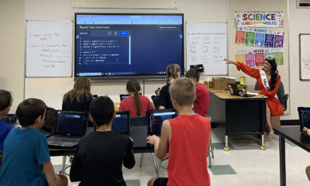
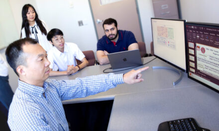
The electrical engineering senior capstone team developing resources for open-source semiconductor design processes poses for a photo on Arizona State University’s Tempe campus. James Doyle, a visiting faculty member and electrical engineering doctoral student, leads the team under the guidance of his doctoral degree mentor, electrical engineering Professor Hongbin Yu. The resources integrate existing open-source software and low-cost manufacturing processes to create an easily accessible workflow to design microelectronics. Photo courtesy of James Doyle/ASU
Aspiring designers of microelectronic chips, also known as integrated circuits, may find their hopes of creating a working chip of their own dashed if they are short on financial resources. According to James Doyle, an electrical engineering doctoral student and visiting faculty member in the Ira A. Fulton Schools of Engineering at Arizona State University, the industry’s dominant suite of chip design programs from Cadence Design Systems can cost $100,000 or more for a single user.
Even those who work full-time and want to pursue chip design on their own would struggle with such a high cost; the average salary for an electrical engineer in the U.S. is $114,050 as of May 2022, according to the U.S. Bureau of Labor Statistics.
Electrical engineers using their companies’ software also run into issues with intellectual property rights. Anything designed using the employers’ program licenses becomes the property of the employer, which limits experimentation.
Doyle set out to overcome this impediment by putting together a suite of open-source chip design tools. While the tools are publicly available for free, they don’t synchronize well with each other and often result in format errors that need to be corrected when transferring the designs and code from one program to the next, further extending a chip’s development timeline.
“We have it so it’s seamless,” Doyle says. “There are no fixes required. That’s a huge step.”
Hongbin Yu, Doyle’s doctoral degree mentor and a professor of electrical engineering in the School of Electrical, Computer and Energy Engineering, part of the Fulton Schools, asked Doyle if the project could serve as a hands-on capstone experience, a requirement for graduating seniors.
“I suggested to Jim the idea could be a capstone opportunity for highly motivated students who would love to work on such a project to apply their skills and knowledge, potentially helping them land a job in the semiconductor field,” Yu says.
Doyle agreed, and he now leads a student team’s design efforts with Yu serving as a faculty mentor.
Streamlining the chip design pipeline
Doyle and his team are developing a single package that will properly format the chip designs and code from one program to the next. Running on the Rocky Linux operating system, the tool flow begins with Xschem, an electronic design automation program.
Once the electronic design automation has been completed, the output is then tested in the ngspice circuit simulator. After the design is tested in the simulator program, it goes to the SkyWater Technology SKY130 PDK development kit. SkyWater is a semiconductor manufacturer.
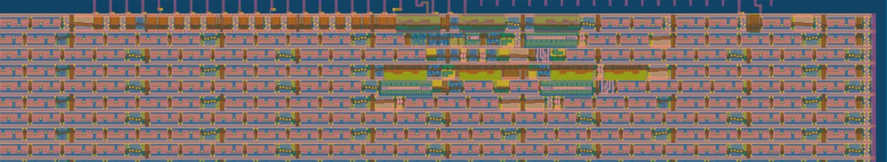
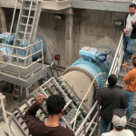
A computer-generated image shows the layout for the capstone team’s first chip. Currently in production, the chip is expected to be ready for testing and further use by the team in February 2024. Their design is available on GitHub. Image courtesy of James Doyle/ASU
The development kit formats everything properly to use a standard design of a SkyWater 130-nanometer chip. The design files are then sent to SkyWater for fabrication.
Once the chip is built, it’s then sent back to those who ordered it. The entire process is completed at a cost of about $100 per chip and can take up to six months to complete the manufacturing process.
Tthe chip is then tested in an Efabless Caravel test harness chip. The Caravel is built to plug into a SkyWater 130nm chip to test its programmed capabilities.
Doyle and his team designed a tool package to create mixed-signal, analog and radio frequency chips, which are typically used in communications technology.
The team’s tool suite will remain installed on a computer in the Engineering Research Center on ASU’s Tempe campus. However, the package will be free to download for anyone with Microsoft Windows 7 and Windows 10 operating systems through the Oracle VirtualBox program, which allows Windows operating systems to run Linux within their environment.
Providing paths for building complementary printed circuit boards
In addition to the chips, the capstone project also focuses on creating robust capabilities at ASU to create printed circuit boards, or PCBs, which can be used as additional components in certain electronic systems. Unlike chips, PCBs aren’t always made from semiconductor materials, and they often perform functions such as connecting various circuit parts.
ASU has the capability to build PCBs on campus in the Engineering Research Center, but Doyle says the process is slow and complicated. To produce the required PCBs, Doyle’s team uses a process with an open-source electronic design automation and simulation program called EasyEDA.
Once designs are completed using EasyEDA, the designs are sent to a company called JLCPCB, which uses EasyEDA integration to accelerate the manufacturing process.
“It’s a complete turnkey system where you capture the schematic and push a button. It does the layout automatically, you push another button, it orders the PCB and you get it in a week,” Doyle says.
To complete the process even faster and entirely on campus, Doyle is investigating if ASU is able to purchase a printer that can produce PCBs from designs in less than an hour, which would further increase accessibility.
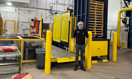
The capstone team built a surface-mount technology assembly station on the Tempe campus to allow them to modify the PCBs after production with the necessary parts such as transistors. Surface-mount technology enables users to add any necessary parts directly to the surfaces of PCBs.
Once the project is complete, the assembly stations will remain on the Tempe campus for students to use in the future.
Developing a future microelectronics workforce through hands-on experience
Dominic Cosentino, a senior undergraduate electrical engineering student, was interested in chip manufacturing but discovered the prohibitive costs of chip design software during his experience at ASU. Once Cosentino learned of the opportunity to join Doyle’s project to make semiconductor chip design open-source, he jumped at the chance to join the project.
Cosentino designed the surface-mount technology assembly for the PCBs to test one of the chips the team designed that is currently in the manufacturing process at SkyWater. The chip will serve as a Gray code counter, which helps ensure reliable and accurate signal transmission in communications technology.
After he graduates, Cosentino plans to become a chip design engineer.
“This project has deepened my interest in integrated circuit design,” Cosentino says. “I am planning to continue in the field and am currently in the process of interviewing for a position.”
After the capstone project is completed, Doyle intends to continue developing the software suite with future capstone teams to expand capabilities to other types of chips. While the open-source software suite is currently set up for the SkyWater 130nm chips, Doyle aims to develop a type of technology called a gigahertz, or GHz, switching power supply, which would use a different type of chip.
Switching power supplies convert electricity between types and voltages as needed for specific uses. Typical radio frequencies used in switching power supplies don’t exceed a few megahertz, or MHz.
One GHz is equivalent to one thousand MHz, and the higher frequency would enable a power supply’s components to become smaller while improving the conversion of power.
Ultimately, Doyle says using open-source software is the only way he’ll be able to afford to complete his doctoral degree thesis without using a company’s software. If a student uses a company’s paid licenses for chip design software, it would be impermissible to use the results for educational purposes.
He is grateful for open-source access resources that allow him to complete his studies and the opportunity to leave a set of tools that will help other ASU students interested in microelectronics manufacturing.


