


Sounding out more efficient semiconductor manufacturing
ASU electrical engineering professor’s company receives SBIR funding from NASA to reduce waste during semiconductor chip manufacturing
 (1)-1920×1080")
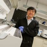
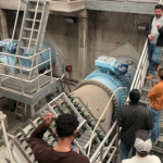
A wafer of semiconductor material is shown in Arizona State University Professor Mariana Bertoni’s lab. Her company, Crystal Sonic, received funding from NASA’s 2022 SBIR Ignite program Phase II to advance their Sonic Lift-off manufacturing technology, which uses sound waves to cut semiconductor wafers for electronic devices. Photo courtesy of Mariana Bertoni/ASU
Current processes to make solar cells and power electronics have a manufacturing waste problem: up to 95% of the initial block of material, known as a wafer or substrate, is destroyed when wafers are extracted from the substrate then thinned out. These semiconductor manufacturing processes are called wire sawing and backgrinding.
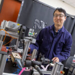
Mariana Bertoni, a professor of electrical engineering in the Ira A. Fulton Schools of Engineering at Arizona State University, and her former doctoral student Pablo Guimerá Coll sought to reduce the waste from wafer manufacturing. They developed a precise method to apply a crack to the semiconductor substrate material with a small amount of force, then use sound waves to accurately guide the crack to cut off only the needed amount.
The resulting clean and accurate cuts allow the substrate material to be used multiple times and eliminate the need for backgrinding altogether, ultimately reducing waste in the manufacturing process.
“I’ve always been fascinated by the process of spalling, even in nature, and the role of vibrations in breaking things,” Bertoni says.
This fascination with vibrations and spalling, a process in which a piece of material is broken off from a larger chunk, resulted in Bertoni and Coll’s manufacturing method, which they dubbed “Sonic Lift-off.” After Sonic Lift-off showed promise, Bertoni and Coll founded Crystal Sonic in 2018 to further develop and commercialize their research.
Bertoni now serves as the company’s chief technology officer, while Coll has since graduated with his doctoral degree in materials science and engineering and is now Crystal Sonic’s research and development director.
Crystal Sonic has continued to gain prominence from its ideas — the company won one of just 12 national $850,000 funding awards from NASA’s Small Business Innovation Research Small Business Technology Transfer Program, known as SBIR and STTR, through SBIR Ignite Phase II for Sonic Lift-off, for which the agency sees potential use to manufacture solar cells that can be used in space. Fellow ASU spinout company Solestial, a business specializing in solar technology for use in space started by ASU electrical engineering alumnus and former Assistant Research Professor Stanislau “Stan” Herasimenka, took home another of the 12 funding spots.
SBIR and STTR programs are offered through all U.S. federal agencies to encourage the development of technology from American small businesses for uses in commercial and government settings. The SBIR Ignite program, started in 2022 and specific to NASA projects, looks to help small businesses by distributing funds on an accelerated timeline compared to lengthier traditional SBIR and STTR processes, allowing the companies to continue their research with minimal disruption and develop their technology more quickly.
Crystal Sonic was one of the first participants of the program and began involvement in SBIR Ignite with a Phase I award, which investigated the feasibility of Sonic Lift-off on large wafers.
Good vibrations
Sonic Lift-off uses a precise application of force to create a crack in semiconductor substrate material. After the substrate is cracked, sound waves guide the crack further into the substrate to create a clean cut through the material, producing a thin semiconductor device used in solar cells or power electronics chip manufacturing.
The technique’s use of sound waves to guide the crack results in a smooth finish, unlike the product from wire sawing, which is rough and requires another step of backgrinding to smooth it to a usable level for consumer devices.
Arno Merkle, Crystal Sonic’s CEO, explains Sonic Lift-off reduces substrate waste by allowing blocks of substrate that are typically used only once to be reused one or more additional times. He says the method’s primary application is for compound semiconductor materials such as gallium arsenide, gallium nitride and silicon carbide.
These materials are commonly used for power electronics applications such as certain types of solar panels and chips that convert electricity and regulate its flow in power grid components and electric vehicle drivetrains and chargers.
“Those kinds of chips are not typically the computer chips you’d think about like the processor in your computer or phone,” Merkle says. “But they are used for other applications like sensors, so even the 3D sensors in your iPhone that measure facial recognition and other sensors for measuring light or distance are examples.”
Because of the difficulty of producing high-quality compound semiconductor materials and the high amount of waste that results from producing chips, devices using them are expensive to produce. Sonic Lift-off’s waste reduction could cut the single largest cost for compound semiconductor chips, which are facing accelerating demand, by at least half.
Lifting off toward the future
While Sonic Lift-off has been proven to successfully cut a bare wafer measuring four inches, the technology has not yet been tested in devices of such a size. Crystal Sonic’s SBIR Ignite Phase II grant will see the company build a second-generation version of the Sonic Lift-off tool and work with manufacturers of space solar technology to determine whether the method can be used in the production of functioning four-inch devices.
Merkle says in the future, Crystal Sonic hopes to process wafers for devices at even larger diameters.
“For things like silicon chips, they’re up to 12-inch wafers right now,” he says. “One of the technical questions we have is, ‘Can we demonstrate this on larger and larger diameter wafers?’”
In the future, Crystal Sonic aims to move on to Phase III of SBIR Ignite, which would see further commercialization of Sonic Lift-off. Merkle says the company plans to start commercialization in the space solar technology industry with potential later market expansion to manufacturers of wide-bandgap semiconductor devices.
With the company’s success and growth as development progresses on Sonic Lift-off, Crystal Sonic has moved out of space rented from Bertoni’s lab on ASU’s Tempe campus into Connect Labs in downtown Phoenix, located in a building created through a collaboration between ASU, development company Wexford and the city of Phoenix.
“We emerged out of ASU’s campus earlier this summer,” Merkle says. “We outgrew that, and we’re hiring two new people to the team. We’re excited to be here in the community of some emerging startups in the Valley of the Sun.”


