


Strengthening semiconductor skills at the SWAP Hub
An ASU-led Microelectronics Commons Hub helps build the workforce and technology needed to secure the US semiconductor future

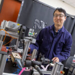
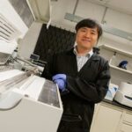
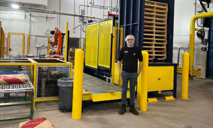
A researcher works with semiconductor materials at Arizona State University’s MacroTechnology Works in Tempe, Arizona. The ASU-led Southwest Advanced Prototyping, or SWAP, Hub, conducts microelectronics research at the facility. The hub is one of eight U.S. Department of Defense Microelectronics Commons Hubs, which aim to accelerate the development of electronic technology and an associated workforce for national defense. Photographer: Samantha Chow/ASU
After the coronavirus pandemic disrupted global supply chains in 2020, a shortage of semiconductor chips developed just as demand for consumer electronics increased from a population stuck at home. At the same time, international tensions increased between China and Taiwan, which produces the majority of the world’s chips.
Electronic chips are essential to international security as well for use in missile systems, fighter jets, tanks, radio communications equipment and more. To meet these needs and more, the U.S. government passed the CHIPS and Science Act, which provides $52.7 billion in funding for U.S.-based semiconductor research, development and manufacturing.
Provisions in the CHIPS and Science Act sponsored the creation of eight Microelectronics Commons Hubs around the country. The hubs aim to boost electronic innovations to advance experimental technology to production for the U.S. Department of Defense, ensuring powerful ideas make it beyond the research lab and into military equipment, while also growing a domestic semiconductor industry workforce.
One of these eight hubs is the Southwest Advanced Prototyping, or SWAP, Hub, an Arizona State University-led research and workforce development consortium of more than 130 partners from academia, government and industry. Hub partners include Sandia National Laboratories, Applied Materials, Northrop Grumman, Intel, NXP Semiconductors and the University of Colorado Boulder.
“The hub is supposed to create an ecosystem,” says Krishnendu Chakrabarty, Fulton Professor of Microelectronics in the Ira A. Fulton Schools of Engineering at ASU and the SWAP Hub’s chief technology officer. “It’s not just about ASU; it’s about the entire country.”
Sally Morton, ASU’s Knowledge Enterprise executive vice president and a professor of statistics, concurs that the hub’s impact will be wide-ranging.
“We are bridging the gap at ASU between research and entrepreneurship by advancing the local semiconductor industry and further enhancing economic competitiveness and national defense,” Morton says. “A shining example is the Southwest Advanced Prototyping Hub, which leverages the collective expertise of our dedicated faculty and students at the Fulton Schools to ensure a vital, sustainable and prosperous future for the area, as Arizona is poised to become the heart of semiconductor research, development and workforce education in the United States.”
Since its announcement in September, the SWAP Hub is now supporting prototyping with six capability areas: circuits, architecture and electrical test; metrology and characterization; power and radio frequency, or RF, electronics; heterogeneous integration; radiation-hardened complementary metal-oxide semiconductor, or CMOS, plus X, or an additional material type, integration; and materials for CMOS plus X integration.
The hub has also identified three themes to define the advances being pursued in microelectronics prototyping: extreme environments, trust and assurance, and workforce development.
Maximizing domestic microelectronics impact
As chief technology officer, Chakrabarty, a faculty member in the School of Electrical, Computer and Energy Engineering, part of the Fulton Schools, oversees the direction of projects’ technical aspects, such as forming research teams, ensuring projects align with DOD needs and identifying hub members with the right expertise for specific tasks. His duties include overseeing the SWAP Hub’s efforts in its capability and theme concentrations. Three Fulton Schools faculty members lead the SWAP Hub’s themes.
- Hugh Barnaby, a professor of electrical engineering, leads the extreme environments theme. The area aims to ensure that electronics can survive harsh conditions, such as high radiation and extreme temperatures, to reflect the tough conditions in which defense technology must operate.
- Michel Kinsy, an associate professor of computer science and engineering, leads the theme of trust and assurance. Because the performance of microelectronics for national defense needs to be trusted and remain robust against malicious actors, efforts in the field seek to ensure supply chain security.
- Binil Starly, a professor of manufacturing engineering and director of the School of Manufacturing Systems and Networks, part of the Fulton Schools, leads efforts in the workforce development theme, which aims to build a workforce for the burgeoning U.S. microelectronics manufacturing industry.
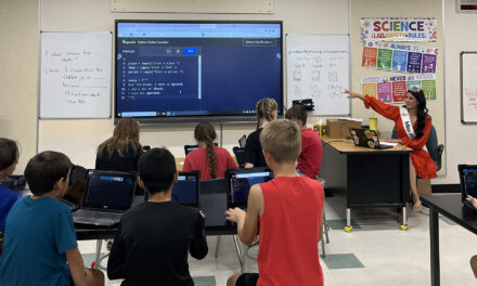
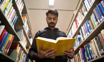
Making a microelectronics workforce
“Academic partners in the SWAP Hub jointly have more than 60,000 degree-seeking students in science, technology, engineering and math, or STEM, majors,” Starly says. “If we target 10% of these students toward a microelectronics industry career pathway, we can positively impact the region’s workforce needs.”
The hub’s workforce development component aims to raise awareness among college students in STEM majors and high schoolers about microelectronics careers to aid national defense efforts. Additional goals include designing educational programs to train microelectronics workers for the SWAP Hub’s technologies of focus and developing extended reality technologies, such as virtual and augmented reality, to enable low-risk, hands-on training.
As the U.S. microelectronics industry rapidly grows, thousands of employees are needed to fill roles in new fabrication facilities. The SWAP Hub aims to bridge the gap through means such as developing stackable credentials with the ASU Learning Enterprise certifying workers in knowledge of rapidly evolving electronics fields.
Starly emphasizes the importance of the SWAP Hub’s partners combining strengths and resources to address various workforce education challenges. He notes ASU has multiple assets to bring to the table, including ASU Preparatory Academy K-12 charter schools, flexible online classes and the MacroTechnology Works, or MTW, research and pilot production facility.
Preparing microelectronics innovations for production
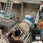
MTW is a former Motorola semiconductor fabrication facility located in the ASU Research Park in Tempe and is now home to an ecosystem of startups, research labs and electronics manufacturing tools perfect for building small batches of full-size electronics prototypes. Jason Conrad, chief operating officer of the SWAP Hub, is also the site lead for MTW, which serves as a major SWAP Hub research facility.
As SWAP Hub COO, Conrad oversees the hub’s day-to-day operations and grows engagement with the Hub’s partners.
“MTW is key to the SWAP Hub’s future,” Conrad says. “I like to call it a crown jewel for ASU.”
He says MTW’s infrastructure, tools and capabilities are a rarity among universities. Chakrabarty believes the resources MTW offers played a major role in the decision to select ASU to lead the SWAP Hub.
A partnership with Applied Materials, resulting in the Materials-to-Fab Center, a partnership with NXP, and Arizona Commerce Authority and CHIPS and Science Act funding are providing more than $200 million in equipment upgrades for MTW. The new equipment will enable MTW to meet increasingly advanced technological demands for adequate performance in various steps of the semiconductor manufacturing process.
“With over $63 billion of private investment in semiconductors in the Phoenix area since 2021, Arizona is becoming a hotbed of semiconductor manufacturing in the U.S.,” Conrad says. “With ASU and the SWAP Hub here in Tempe, we are able to take advantage of the vast network of partners locally as well as regionally across the Southwest.”
The new equipment at MTW is enabling the exploration of the SWAP Hub’s six capability goals.
Expanding electronics capabilities to secure the future
Faculty members across the Fulton Schools are contributing to efforts within the SWAP Hub to advance microelectronics manufacturing — from optimizing materials to packaging.
Sule Ozev, a Fulton Schools professor of electrical engineering, leads the circuits, architecture and test capability, which focuses on design and test capabilities to advance microelectronics.
The metrology and characterization capability, headed by Umberto Celano, a Fulton Schools associate professor of electrical engineering, analyzes microelectronics’ physical, chemical and electrical properties.
Trevor Thornton, a Fulton Schools professor of electrical engineering, leads the power and RF electronics capability, analyzing novel materials and designs for communications and power electronics.
Heterogeneous integration, a capability headed by Christopher Bailey, a Fulton Schools professor of electrical engineering, seeks to find best practices for integrating components to form electronic systems consisting of combinations of multiple smaller chips.
Radiation-hardened CMOS plus X integration investigates the addition of other materials to CMOS chips, which are a type of semiconductor common in modern electronics.
Radiation-hardened CMOS chips have proven to be robust against radiation exposure. The radiation hardening ensures greater function in high-radiation environments such as space. The researchers also plan to analyze and test the performance of new devices in various environmental and radiation conditions.
The capability will take advantage of Sandia National Laboratories’ facilities and Sandia researcher Sapan Agarwal’s radiation hardening expertise. Agarwal will lead the efforts with his former colleague Matthew Marinella, a Fulton Schools associate professor of electrical engineering who joined ASU from Sandia.
Seth Ariel Tongay, a Fulton Schools professor of materials science and engineering, leads the capability for development of new materials and their CMOS plus X integration. Tongay, a faculty member in the School for Engineering of Matter, Transport and Energy, part of the Fulton Schools, heads investigation of large-scale manufacturing methods for CMOS chips with emergent semiconductors.
Tongay says the manufacturing challenge will be to effectively manufacture these emergent semiconductors and integrate them with state-of-the-art CMOS templates at temperatures low enough not to damage them. Tongay and his team aim to accomplish goals such as the development of neuromorphic computing devices that allow processing of various information at the same time like a human nervous system and manufacturing semiconductors for infrared detectors.
He believes Arizona will rise further to national microelectronics prominence through the SWAP Hub’s work.
“The SWAP Hub places Arizona on the map where exciting things happen, and these exciting development projects benefit our nation’s interests,” Tongay says. “It will bring a highly skilled workforce to increase Arizona’s manufacturing and electronics ecosystem.”
Ramping up to SWAP electronics expertise
The SWAP Hub gained such national attention with a visit from DOD representatives in January 2024. They toured ASU facilities and viewed presentations to stay informed on the hub’s plans.
Part of those plans include prototyping project ideas submitted to the DOD’s latest request for proposals for funding. The hub was allowed to submit only 15 plans; among those submitted by hub partners, the hub leadership had to whittle down the finalists from more than 75 submissions.
“Our faculty are all in in a big way,” Chakrabarty says. “We have been able to get the ASU community excited about this.”


