


Taking semiconductor manufacturing to new heights
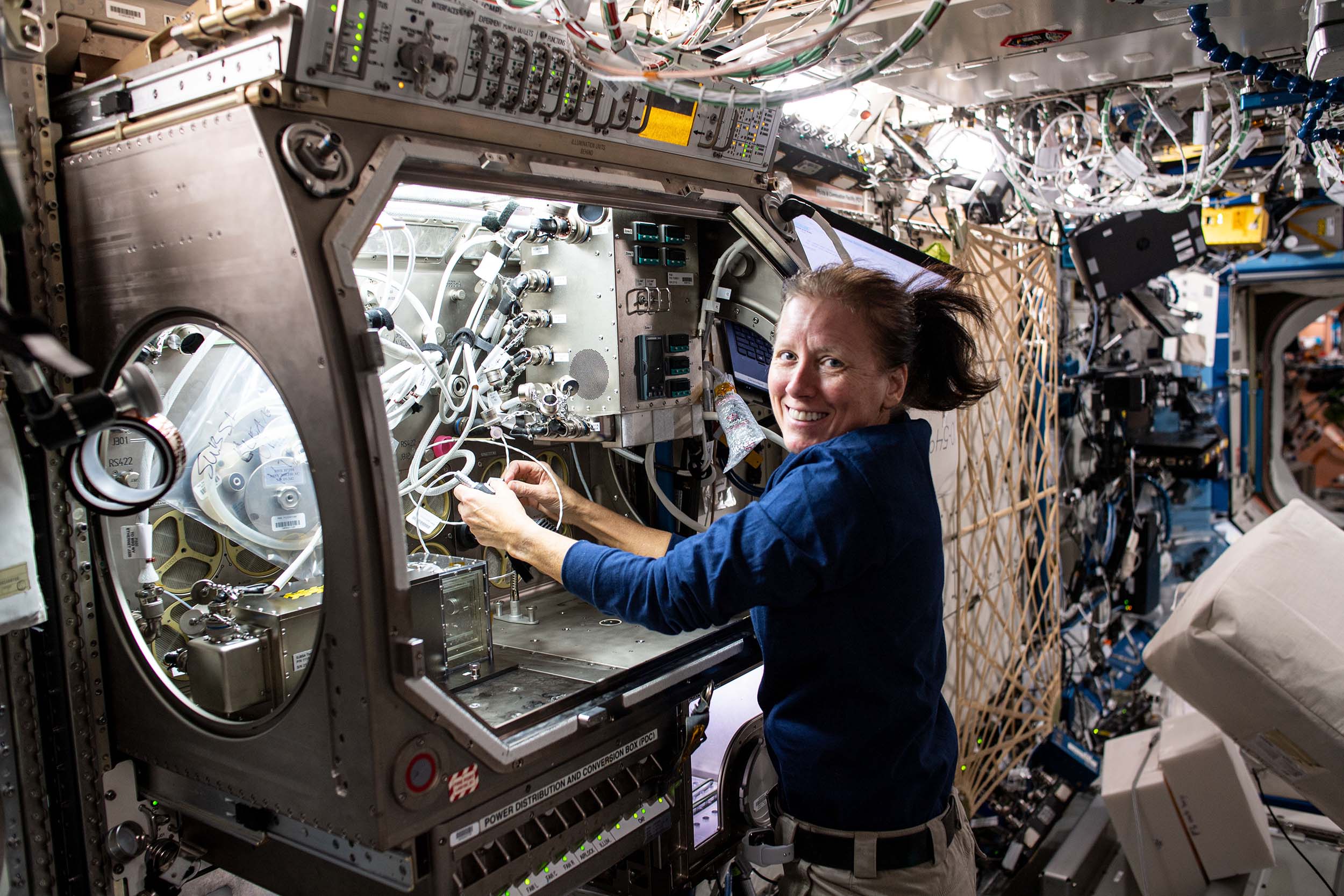
ASU researcher Ying-Chen “Daphne” Chen is working with collaborators on a NASA project to manufacture microelectronics in space

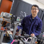
Assistant Professor Ying-Chen “Daphne” Chen stands in front of a screen displaying an image of the moon while holding semiconductor material reflecting a model of the Earth. Chen is working with collaborators at NASA and in industry and academia to develop a manufacturing method for microelectronics in microgravity environments, reducing resources needed to build the devices. Photo by Erika Gronek/ASU
Factories floating in space sound like science fiction, but they may not be far off in the future. Ying-Chen “Daphne” Chen, an assistant professor of electrical engineering in the Ira A. Fulton Schools of Engineering at Arizona State University, is working as a co-primary investigator on NASA research with academic and industry collaborators to build a blueprint for building semiconductor devices in space.
Manufacturing microelectronics in space has the potential to eliminate key lengthy and costly steps in the semiconductor manufacturing process, specifically for 3D oxide-based resistive random-access memory, or RRAM, devices used on Earth. These 3D devices differ from traditional 2D RRAM devices by stacking layers of memory storage cells vertically instead of a traditional flat arrangement, allowing for a smaller footprint and more memory storage in a single device.
The team’s research is financed by funds from the CHIPS and Science Act and NASA’s In Space Production Applications program. Led by Principal Investigator Curtis Hill, a senior materials engineer at NASA, the project intends to harness the reduced pressure from microgravity in space to eliminate the need for etching, a step in which trenches are deepened in a chip’s surface to make sufficient room for its conductive metal contacts.
Etching is required in Earth-based semiconductor manufacturing processes due to the need for a thicker layer of semiconductor wafer thin film material to compensate for pressure from gravity. The researchers hypothesize a slimmer thin film layer can be used in space due to the lack of gravity, resulting in a trench already made deep enough during manufacturing to render etching unnecessary.
“To manufacture a chip, companies normally need many steps in a clean room on Earth,” says Chen, a faculty member in the School of Electrical, Computer and Energy Engineering, part of the Fulton Schools. “The goal for this project is to realize ‘all-in-one’ printing with a printer capable of manufacturing 3D stacking structures, active layers and metals.”
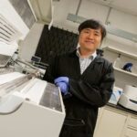
A researcher sets up manufacturing equipment for an experiment in space to see how microgravity affects the solidification of brazing alloys. Photo courtesy of NASA
Using these semiconductor printing devices, which have a much smaller footprint than a fabrication facility on Earth, would reduce the time needed to manufacture a 3D RRAM device and do away with the need for large amounts of personal protective equipment. There is interest in the method from a variety of industry collaborators, including Tokyo Electron America, Axiom Space, Intel and Fujifilm, all of which are involved in the research.
“For future commercialized manufacturing, more transportation companies will join space shipping efforts, reducing cost and increasing competitiveness,” Chen says. “I see many of these technologies, or high-speed automated versions of them, eventually in small low-Earth orbit factories to build a semiconductor ecosystem in space for chip manufacturing and characterization.”
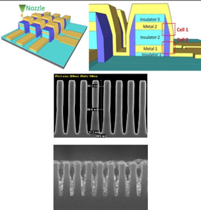
A diagram shows the type of devices Chen and her collaborators intend to experiment with building in space. The test devices, which have already undergone an etching process, will have a special ink injected into their etched trenches to determine the ink’s effectiveness in the manufacturing process. Graphic courtesy of Curtis Hill/NASA
Semiconductors from commercial space stations
The research team, which includes Iowa State University Associate Professor of materials science and engineering Shan Jiang and University of Wisconsin–Madison Assistant Professor of industrial and systems engineering Hantang Qin on the academic side, will conduct the first test of their semiconductor manufacturing theory with a parabolic flight conducted by aviation company Zero-G that will provide 20 seconds of zero-gravity conditions.
A microelectronics manufacturing printer will be installed on the plane before takeoff and will be activated once zero-gravity conditions are achieved. It will then print a semiconductor device within those 20 seconds. The flights are scheduled to take place in October.
If the research proves successful, it opens the door to installing semiconductor printing devices on the International Space Station as well as future commercial space stations like the one planned by Axiom Space. Floating factories attached to larger space stations in orbit are also a possibility.
Hill says the research intends to develop the manufacturing method to enable industry to regain U.S. electronics industry prominence.
“We strongly believe the use of low-Earth orbit and microgravity is a game-changing technology that will enable the U.S. to take the lead in semiconductor manufacturing,” he says. “We hope to ultimately drive the advancement of the U.S.’ semiconductor manufacturing ability and to develop a space economy for it.”
Hill chose Chen for the project due to her expertise in next-generation memory devices, which resulted in her leading the project’s manufacturing methods. As a first-time collaborator with ASU, Hill says he’s impressed with the experience so far and hopes to continue collaborating with the university on future projects.
“I really enjoy working with Dr. Chen,” he says. “She’s enthusiastic and brings a positive approach. Researchers like her, who are optimistic and always looking for advantages and things to help the team, are a great asset.”


