


Perfecting semiconductors for power electronics
Nidhin Kurian Kalarickal collaborates with industry to develop damage-free manufacturing methods for microelectronics

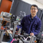
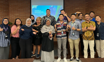
An electric U-Haul van has its hood open for onlookers to view at an event on the Arizona State University Tempe campus. Nidhin Kurian Kalarickal, an assistant professor of electrical engineering in the Ira A. Fulton Schools of Engineering at ASU, has developed a damage-free semiconductor manufacturing step known as etching for emerging material gallium oxide. Gallium oxide has applications in areas such as power electronics for electric vehicles. Photographer: Erik Wirtanen/ASU
As the world becomes increasingly electrified, the need for power electronics is greater than ever. Power electronics use semiconductors to regulate the flow of electricity, converting it between needed types and voltages for specific uses.
Gallium oxide is an emerging material with great potential for power electronics. However, methods for a manufacturing step called etching, which turns gallium oxide into usable power electronics chips, have a problem: They damage the material.
While the resulting product is still usable, the damage changes gallium oxide’s electrical properties, meaning electronics using the compound are unable to achieve their maximum performance.
Nidhin Kurian Kalarickal, an assistant professor of electrical engineering in the Ira A. Fulton Schools of Engineering at Arizona State University, solved this problem by developing a damage-free etching process with his graduate materials science and engineering student, Abishek Katta, and collaborators from semiconductor manufacturing equipment company Agnitron Technology.
Carving a new path for semiconductors
Gallium oxide has applications in power electronics requiring high amounts of voltage such as electric cars and trains, power grid technology and motors used in industrial equipment. The compound is part of an emerging class of materials known as ultra-wide bandgap semiconductors, which provide less resistance against the electricity moving across them than traditional materials such as silicon.
Due to the lower resistance resulting in greater efficiency, power electronics built from ultra-wide bandgap materials can convert and channel the same amount of power or more than conventional materials in a smaller, lighter package.
However, some of gallium oxide’s inherent advantage is lost during the semiconductor manufacturing step of etching. During etching, material is removed from the initial wafer of the semiconductor to create patterns. Etching enables other components of a device, such as circuitry, to be installed.
Traditional etching of gallium oxide is done using the standard process of plasma-based reactive ion etching and uses gases such as chlorine and argon. The process involves exposure to energetic plasma, which damages gallium oxide, creating surface and sub-surface defects and reducing its power conversion capabilities.
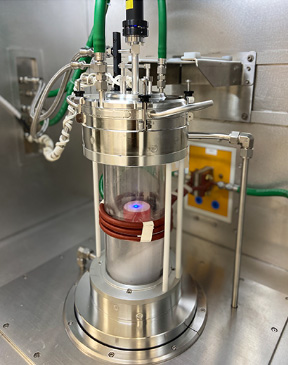
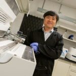
A metal-organic chemical vapor deposition, or MOCVD, reactor from Agnitron used by Nidhin Kurian Kalarickal in his gallium oxide etching research. Photo courtesy of Nidhin Kurian Kalarickal/ASU
Collaborating with industry to destroy damage risk
To remedy the damaging methods, Agnitron representatives approached Kalarickal, a faculty member in the School of Electrical, Computer and Energy Engineering, part of the Fulton Schools, and discussed developing a new etching process after ASU purchased a metal-organic chemical vapor deposition, or MOCVD, reactor tool from the company. The tool is used for growing semiconductor material such as gallium oxide.
“Agnitron wanted to engage with my team, and the company’s representatives were quite interested in the idea of investigating in situ etching using metal-organic precursors,” Kalarickal says.
Kalarickal and Agnitron’s method differs from traditional ones in that it uses the same basic metal-organic compound, triethylgallium, that is also used for the growth of gallium oxide in the presence of oxygen. Other methods use a different material that involves damaging energetic plasma.
When gallium oxide is heated and exposed to triethylgallium in the absence of oxygen, gallium oxide undergoes a chemical reaction, resulting in the formation of gallium suboxide. Gallium suboxide is volatile and easily escapes from the sample surface, resulting in etching.
Kalarickal’s method does not involve energetic plasma, eliminating the damage that occurs to gallium oxide from traditional processes. The new technique can be completely performed within a MOCVD reactor, making it possible to etch and grow gallium oxide without exposure to the ambient environment.
Providing a student research opportunity
The work with Agnitron provided Katta, a master’s degree student who has studied under Kalarickal since the spring 2023 semester, with hands-on research experience. Katta processed material samples in ASU’s NanoFab and Eyring Materials Center semiconductor fabrication facilities and analyzed them.
Katta’s experience proved to be a steppingstone for further efforts in his research career. Since finishing his work on the in situ etching project, he participated in the Fulton Schools Master’s Opportunity for Research in Engineering, or MORE, program and gained a TSMC AZ Fellowship.
“I truly appreciate the opportunity given by Dr. Kalarickal to a master’s degree student to work on and contribute to the in situ gallium etching work,” Katta says. “It showed me what it is like working on cutting-edge research and contributing to the scientific community. Working with Dr. Kalarickal has been both inspiring and intellectually rewarding.”
In addition to his fellowship and MORE program spot, the work also led to a full-time job offer for Katta from TSMC.
Powering the future of gallium oxide electronics
Since the in situ method’s development, Kalarickal and his collaborators have worked on two scientific journal papers related to the project. One has been accepted for publication in the Journal of Applied Physics, while the other is almost complete for submission.
The in situ etching process has already been put into practice as well. Doctoral students in Kalarickal’s research group are using the method to develop high-performance power electronic devices, charging up the field for an electrically powered future.


