


New semiconductor material shows promise for more efficient power electronics
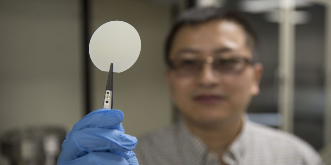
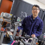
Above: Professor Yuji Zhao is working to advance fundamental knowledge of selective area doping processes for gallium nitride wide-bandgap semiconductors. Photographer: Pete Zrioka/ASU
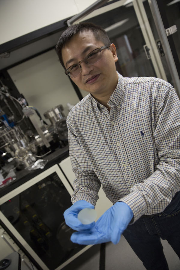
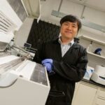
Yuji Zhao and his team are taking an innovative, advanced materials science research approach. Photographer: Pete Zrioka/ASU
Every year it seems like we have another device to charge — laptops, smartphones, tablets, wearable electronics, electric cars and so on. Charging processes ubiquitously use power electronic switches to convert electricity from one form to another so that it can be used in these devices. As power electronics become increasingly part of how we move and consume electricity, the U.S. Department of Energy (DOE) is looking for new ways to make these devices more powerful, more efficient and more compact.
Semiconductors are a critical part of power electronic devices, which today, are most commonly made of silicon semiconductor. However, silicon gets less efficient as power demands increase, so new materials are needed as power electronics capabilities and performance continue to advance. Gallium nitride (GaN) is a promising new wide-bandgap (WBG) semiconductor material with properties that allow it to operate at higher voltages, frequencies and temperatures at higher efficiencies than silicon.
To achieve semiconductor power devices, specific impurities are added to the semiconductor materials to achieve structures called p-n junctions through a process called doping. However, the lack of effective doping processes for GaN WBG semiconductor materials currently obstructs the progress in creating these new and better power electronics devices based on these materials.
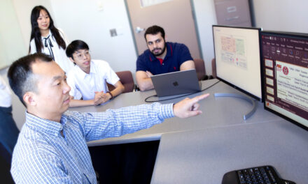
Yuji Zhao, assistant professor of electrical and computer engineering at Arizona State University’s Ira A. Fulton Schools of Engineering, is working to advance fundamental knowledge of selective area doping processes for GaN WBG semiconductors through a $1.5 million project selected by the DOE Advanced Research Projects Agency-Energy (ARPA-E) as part of its Power Nitride Doping Innovation Offers Devices Enabling SWITCHES (PNDIODES) program. The PNDIODES program aims to address technological gaps in GaN doping, a critical technical step to achieve high performance GaN power devices.
“We need to get a fundamental understanding of the critical issues for the p-n junction doping, why it’s not effective, and what effective approach we can use,” Zhao says. “We’re also developing a new method to achieve a GaN vertical power transistor that can meet ARPA-E’s target including current, breakdown voltages, efficiency and more.”
Zhao’s team — comprised of co-principal-investigators Stephen Goodnick, professor of electrical engineering, as well as Robert Nemanich and David Smith, both ASU Regents’ Professors of physics, and Fernando Ponce, professors of physics — is taking an innovative, advanced materials science research approach to this problem. Their project, “Effective Selective Area Doping for GaN Vertical Power Transistors Enabled by Innovative Materials Engineering,” is one of seven projects from academia and industry selected for the new ARPA-E PNDIODES program launched in June.
The GaN WBG semiconductor device the team is developing has a new vertical format, and thus has different p-n junction structure. Zhao believes their approach to GaN WBG semiconductor development is what impressed the DOE.
“We have a lot of innovative ideas that have never been explored,” Zhao says. “We have a very comprehensive approach that covers physics to materials to the device.”
He also credits his “dream team” of ASU researchers to their success in earning ASU’s award from the program.
“We have a very strong team with a recognized track record in GaN materials and devices and organized effort from experts all around,” Zhao says.
The School of Electrical, Computer and Energy Engineering, one of the six Fulton Schools of which Zhao and Goodnick are faculty members, has heavily invested in Zhao’s research, including the multi-million-dollar Metal-Organic Chemical Vapor Deposition Lab on ASU’s Tempe campus.
“This is a very big investment from the Fulton Schools, and we have been given support from the Fulton Schools and ASU to organize this effort so we can put people like Bob Nemanich, Fernando Ponce and David Smith together so we could submit this proposal.”
With several other proposals pending in GaN research, Zhao and the team are looking to continue their momentum beyond this ARPA-E project.
“We think this is going to be something big, and this is a good starting point,” Zhao says. “We’re going to take advantage of this winning proposal and we hope to turn this into a new research center in the near future.”


