


A new low-cost method to mass manufacture nanomaterials
ASU researcher introduces new method for electrochemical nanoimprinting
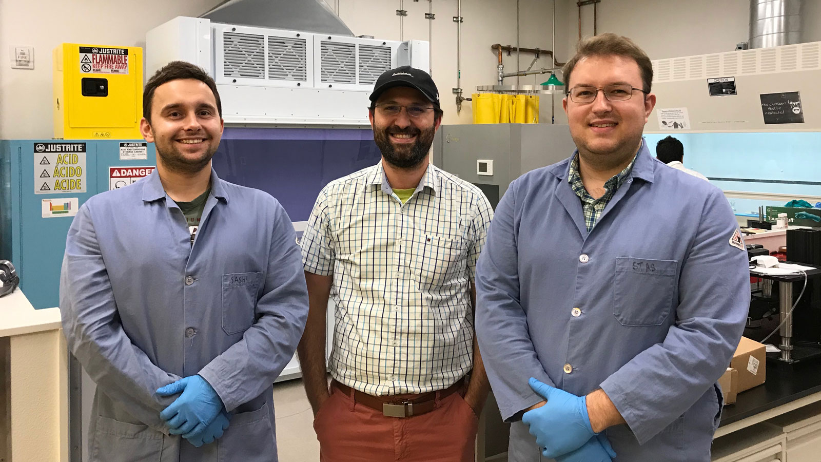
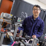
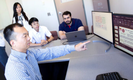
Above: Assistant Professor Bruno Azeredo (center) and materials science and engineering doctoral students Aliaksandr Sharstniou (left) and Stanislau Niauzorau (right) recently co-authored a paper that introduces electrochemical nanoimprinting as a new, low-cost method for large-scale production of single-crystal semiconductors. Photo courtesy of Bruno Azeredo
The emerging field of nanotechnology has spurred many advances in energy, defense and medicine applications.
Nanomaterials have unique and rewarding chemical, physical and mechanical properties, from enabling superhydrophobic and self-cleaning windows to enhancing absorption and efficiency of photovoltaic cells. In an ideal world, nanomaterials would be everywhere, but they often don’t appear in our lives.
The disparity lies somewhere between research and commercialization where the costs of nanomaterial production don’t scale favorably. There’s limited ability to mass manufacture nanomaterials with quality control, resolution and low-cost.
The need for new methods to mass manufacture nanomaterials has led Arizona State University Assistant Professor Bruno Azeredo to study the physics of nanomaterials’ processing and find solutions to this problem.
Azeredo, a faculty member in the Ira A. Fulton Schools of Engineering at ASU, co-authored a paper published May 9 in the Proceedings of the National Academy of Sciences of the United States of America. The paper introduces electrochemical nanoimprinting as a new, low-cost method for large-scale production of single-crystal semiconductors, such as silicon.
He shares his thoughts on electrochemical nanoimprinting and some of his research findings.
Q: Explain your research on electrochemical nanoimprinting.
A: In traditional manufacturing operations, like coin manufacturing, a material is heated to be formed into a shape. We take metal disks (blanks) and imprint them with a hard die (forming). The pressure of the die, or mold, at high temperatures allows the metal to flow into the shape of the die.
In nanomanufacturing, this concept has been miniaturized down to the nanoscale, particularly for metals and polymers by a process called nanoimprinting lithography. This process works with the same principle as coin manufacturing but can create features as small as 10 nanometers! However, nanoimprinting lithography doesn’t work for inorganic single-crystal semiconductors because they recrystallize and degrade during heating cycles and become almost useless.
We went on a journey to imprint semiconductors, particularly silicon, without the use of combined heating and imprinting. We found it could be done with electrochemistry, and we called it electrochemical nanoimprinting (Mac-Imprint).
In Mac-Imprint, a mold, or stamp, is coated with a thin-film catalyst and brought into contact with a silicon wafer while immersed in a wet etchant (the chemical used to etch designs into metal). Upon the catalyst-coated stamp contacting the silicon surface, the silicon substrate is selectively corroded and etched at the contact points only. As the etch evolves, the silicon substrate takes the form of the stamp. This process is analogous to coin manufacturing, except we etch the silicon instead of using forming techniques.
Q: What does this process do that current processes can’t do?
A: Mac-Imprint has wafer-scale patterning capability and sub-20-nanometer shape accuracy in three dimensions. The stamps/molds may be reused numerous times for mass manufacturing. Mac-Imprint is compatible with roll-to-roll (R2R) nanomanufacturing — a process used to create electronic devices on a roll of flexible plastic or metal foil — and uses low-cost tooling and Earth-abundant consumables.
The use of consumables gives electrochemical nanoimprinting the potential to be very inexpensive and extendable to an R2R configuration for large-scale production formats. Additionally, this technique is extendable to other semiconductor materials and formats, such as amorphous silicon films and III-V semiconductors.
Q: Does this method open up new avenues for circuit fabrication?
A: Mac-Imprint enables researchers to manufacture 3D microstructures and nanostructures onto silicon with nanometer precision and shape accuracy via a low-cost approach.
This new capability enables prototyping complex 3D devices/surfaces, which will have a cascade effect in many research areas where 3D nanopatterning is critical such as nanophotonics, silicon photonics, biosensing and photovoltaics.
Particularly, we are interested in silicon photonics and free-form optics for making advanced optical devices like infrared lenses, optical interconnects, waveguides and collimators.
Q: How can electrochemical imprinting be used in the future?
A: We can’t benefit from nanotechnology if we don’t invent processes for mass production of nanomaterials. The technique we invented for nanopatterning of silicon may be employed in the manufacturing of the high-speed optical interconnects used in data centers.
The increase in speed to transmit signals will allow for more high-speed connections and lead to a more interconnected world.


