Using sapphire for biosensing: A new way to shape the gemstone
ASU researchers demonstrate the first sapphire-supported nanopore membrane with improved cost-effective, low-noise performance over conventional silicon-based platforms for biomolecular sensing.
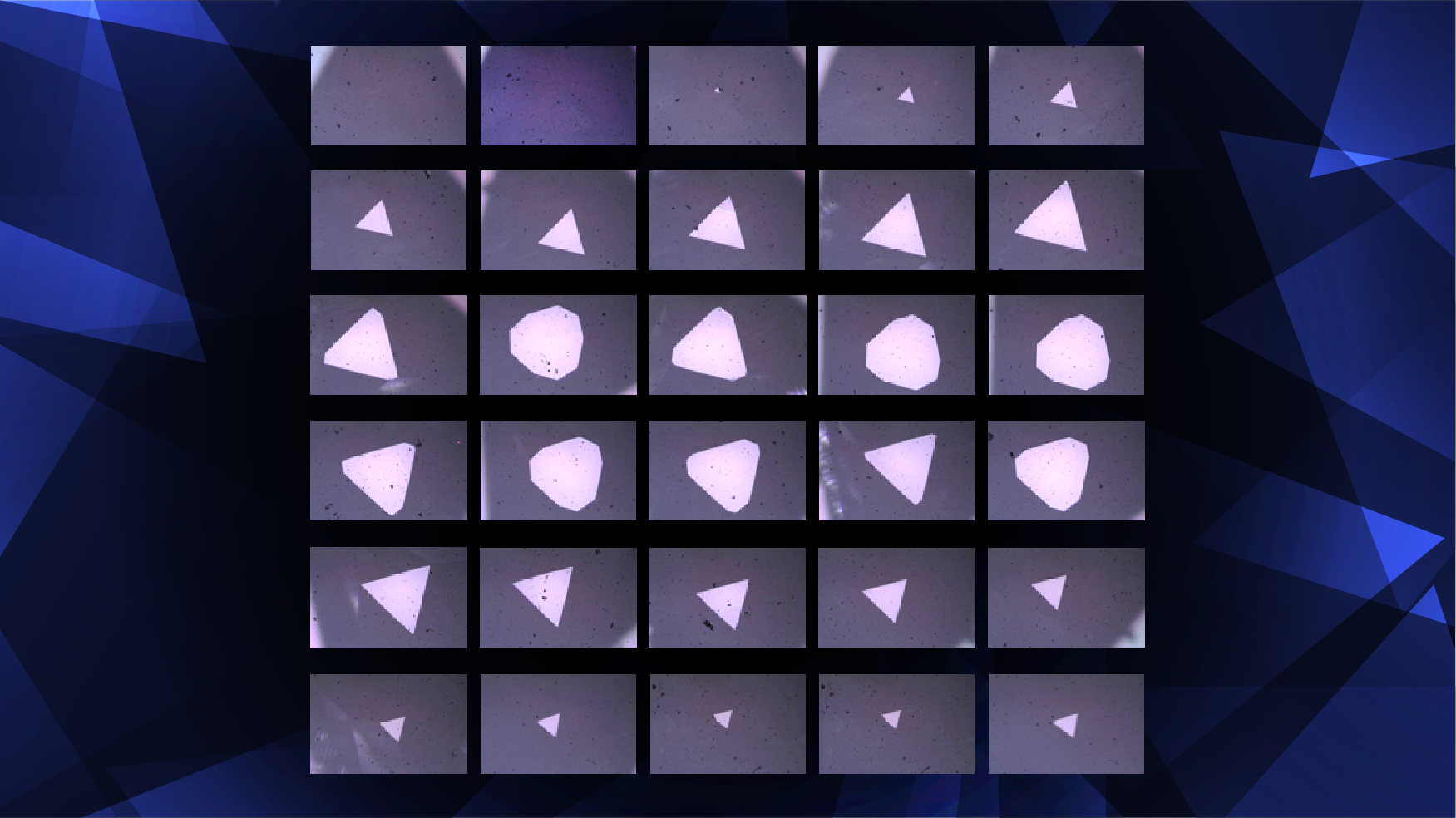
Above: Experiments into using sapphire crystals resulted in the first demonstration of low-noise, cost-effective triangular nanoscale membranes for nanopore sensing and micro-electromechanical system, or MEMS, applications. The work was led by Arizona State University Assistant Professor Chao Wang and his multidisciplinary research team to create the scalable manufacturing process for high-performance biosensors. Graphic by Connor McKee/ASU with images courtesy of Chao Wang
Boiling acid and sapphire crystals sound like the makings of mythological magic. But the two are the key components of a new cost-effective, high-quality and scalable membrane fabrication process.
ASU researchers have developed the first process to successfully use sapphire — not the blue gemstone but transparent and crystalline wafers used in microfabrication — for nanopore membrane manufacturing.
The process was first demonstrated by Chao Wang, an assistant professor of electrical engineering in the Ira A. Fulton Schools of Engineering at Arizona State University, and his research team at ASU. The results of their research were recently published in a paper titled “Sapphire-Supported Nanopores for Low-Noise DNA Sensing” in the research journal Biosensors and Bioelectronics.
The new process will help create low-noise, solid-state sapphire-supported nanopores that can be used for higher-speed DNA sensing and even virus detection, among other biosensing applications. It can also be used for micro-electromechanical system, or MEMS, applications like the tiny sensors that drive motion-sensing features in smartphones.
The development of the new manufacturing process is four years in the making and was demonstrated in the NanoFab and Eyring Materials Center at ASU.
The process involves a crystalline sapphire substrate sandwiched between two layers of silicon oxide. The top layer of silicon oxide has a triangular hole serving as a “mask” to guide boiling sulfuric and phosphoric acids to etch into the sapphire until only a thin triangular membrane is left.
Swapping silicon for sapphire
Artificial membranes and nanopores are based on cells. The outer layer of a cell is a membrane with tiny pores that allow in certain molecules the cell needs. These biological nanopores are about 1 nanometer wide — in comparison, a sheet of paper is about 100,000 nanometers thick.
Their artificial equivalents, called solid state nanopores, are often made of silicon oxide or silicon nitride with a nanometer-scale pore. When used as sensors, nanopores involve an electric current that helps learn information about the properties of a molecule, protein or DNA strand that passes through the pore.
Silicon is widely used for applications like nanopore membranes because it is the go-to material for many established nanoscale manufacturing processes. Its crystalline structure also allows anisotropic (directional) etching in bulk micromachining of suspended membranes, which are used in a variety of sensors.
However, silicon conducts electricity. When used for nanopore sensors the silicon serves as a conductive terminal to create a very large capacitance at the solid/liquid interface, which produces serious background noise that can obscure the electric signals the sensor is trying to detect. What is worse, the capacitive noise increases dramatically with the signal readout frequency, meaning a desired high-resolution and high-throughput data collection must battle the high noise that accompanies serious errors.
To reduce noise and errors, scientists have looked for alternatives to silicon. Glass is an insulator and does not conduct electricity, but it’s much more difficult to manufacture reliably and at high throughput at the nanoscale needed for nanopores. Sapphire is another insulator material used in some high-speed electronics, but it hasn’t been used as a membrane platform before due to its known resistance to many chemicals.
Over the past several years, Wang and his research team explored crystalline sapphire and a new process of creating sapphire-supported nanopore membranes through wet and anisotropic (directional) etching in a concentrated acid bath that is compatible with batch processing.
“This is the first time using sapphire to support the membranes because etching sapphire is nontrivial,” Wang says. “You have to use boiling acids for many hours. The process could look very intimidating. It took us a year to establish a process to handle this safely while etching sapphire at a high enough rate.”
Building on years of research
When Wang started his master’s degree, he worked on making membranes on silicon for MEMS devices. As a doctoral student, he developed the technology to etch sapphire crystals with boiling sulfuric and phosphoric acids for performance-enhanced LEDs. Then as a postdoctoral scholar working at IBM, he worked on nanopores and began to understand the noise issues associated with silicon-based nanopores.
The new sapphire-based nanopore membrane platform technology combines all of Wang’s previous research experience to create low-noise sensors for nanopores and MEMS applications.
Membranes are created by etching down into a material until only a thin layer remains. Just as it’s easier to split wood along its grain, the researchers must work with the crystalline structures’ geometric shape for precise control of the etching rate and the eventual membrane dimensions. For the same reason, glass, an amorphous material, is very difficult to work with.
Silicon crystals are essentially cubic and therefore work best when square membranes are formed, but sapphire crystals are hexagonal. Because of their different structures, the research team determined the sapphire etching needs to work with a new shape: triangles.
Wang’s team designed a secure and effective customized acid etching setup and designed the triangular etching mask used to create uniform membranes in the sapphire’s unique structure.
Pengkun Xia, a graduate research associate and electrical engineering doctoral student working in Wang’s Nanoscience and Biotechnology Lab, helped to investigate and develop the optimized fabrication process for the nanopore membranes on sapphire.
“Due to the complex hexagonal lattice nature of sapphire crystal, the etching of sapphire is not as easy as we expected,” Xia says. “We made great efforts of empirical study to set up a model to demonstrate the scalable formation of small membranes, thus low-noise nanopore chips, on the sapphire wafer.”
To create a consistent triangular shape in the sapphire, the team rotated the triangular window for etching from 0 degrees to 60 degrees along the crystalline structure. This experiment led to membranes that ranged from three-sided shapes up to nine-sided shapes (nonagons) and back down to three-sided shapes.
“Through this analysis we know how the etching process behaves and how to control the shape,” Wang says. “Understanding the impact of crystal alignment on etching with a triangular membrane is very new. The shape is potentially structurally stronger and we have seen that the more edges you have the more fragile the membrane is.”
The resulting membranes demonstrated the feasibility of scalable formation of less than 25-micron (25,000 nanometers) membranes with a size deviation of less than 7 microns over two 2-inch wafers. For accurate sensors, the sapphire chips have much better manufacturability than glass and even manually processed silicon chips that have to add many extra steps, and have comparable or better noise levels.
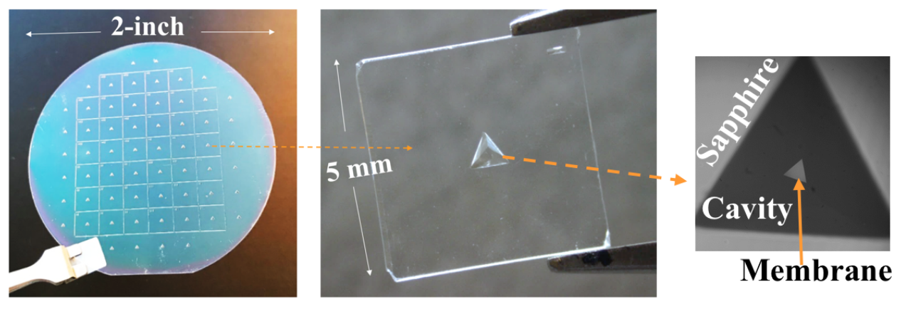
Chao Wang and his research team demonstrated the feasibility of creating triangular sapphire membranes from 2-inch wafers in a scalable manufacturing process. Images courtesy of Chao Wang
Electrical engineering graduate students Jiawei Zuo, Shinhyuk Choi, Xiahui Chen, Md Ashiqur Rahman Laskar and Jing Bai, postdoctoral fellow Pravin Paudel, and Research Scientists Weisi Song and JongOne Im also contributed to the published paper.
Scalable, cost-effective manufacturing
The sapphire manufacturing process is also highly scalable, like that for silicon, because it can be used in wafer-scale batch processing. Hundreds of the membrane devices can be created on a two-inch sapphire wafer, and 10 wafers can be etched in a single wet etching compartment, meaning thousands of membrane devices can be made at the same time to reduce cost. By choosing a specific sapphire crystal orientation on the wafer, as Wang’s team has shown, the etching process is precise and consistent.
“The superior manufacturability plus its low noise level makes the sapphire-supported nanopores competitive over the state-of-the-art nanopore chips available in the market and in labs,” says Xia, who presented the research at the 34th IEEE International Conference on Micro Electro Mechanical Systems.
Once the membranes are created, a separate process can be used to drill a small hole, or nanopore. Or it can be used to create MEMS devices by adding additional mechanical and electrical components.
“Our demonstrated scalable manufacturing of the membrane architecture on sapphire may serve to inspire new designs in MEMS and optoelectronic devices (electronics which use and control light),” Xia says. “I am really looking for this new technology to replace and be superior to the prevalent silicon-based solid-state nanopore sensors in the market in most of the aspects.”
DNA, diseases and data
The sapphire-based platform can be used for a variety of sensing applications.
Nanopores can be used to detect cancer and other genetic diseases in DNA as well as antigens for identifying diseases, like the SARS-CoV-2 coronavirus that causes COVID-19. They can also be used to detect proteins and antibodies, which is a challenging task due to the small size of proteins and typically fast signals — which requires low baseline noise at high recording bandwidth.
“We are hoping solid state nanopores can do DNA, RNA, protein and environmental particle detection like COVID-19 particles,” Wang says. “Nanopores could be used to identify SARS-CoV-2 coronavirus particles or other biological entities.”
Another application is in cryptographically secure DNA-based storage used for data encryption, storage and retrieval. This technology involves long “staple” strands of DNA that are folded into a nearly endless number of structural patterns like origami by matching base pairs of the four nucleotides (A, G, C and T). Shorter staple strands are added to guide the folding and hold it into place. Sapphire-based nanopores will help improve DNA sequencing needed to read the DNA structure patterns.
Now that Wang and his research team have developed the membrane platform, they are hoping to demonstrate its use for DNA memory, protein sensing and other systems with two National Science Foundation grants.
“Imagine you can read DNA and proteins on a USB dongle-sized device, insert that into a computer and get information,” Wang says. “That can be quite impactful.”


