


ASU microelectronics workshop addresses national effort to develop workforce
Leaders in industry, government and higher education discuss shared vision for advancing microelectronics talent pipeline

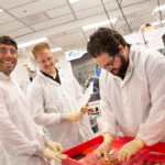
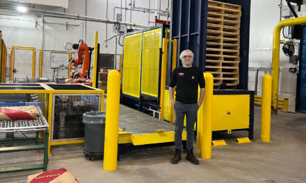
ASU Associate Professor Zachary Holman (left) leads a tour through the Swift Coat lab space at the MacroTechnology Works facility at the ASU Research Park in Tempe. The tour is part of the two-day Microelectronics Education and Workforce Development Workshop for representatives from government, universities, national research labs and private industry gathered to discuss workforce needs. Photographer: Charlie Leight/ASU News
This week, microelectronics leaders from across the nation came together for the 2023 Microelectronics Education and Workforce Development, or MEWD, Workshop, which highlighted the importance of improving semiconductor research, development and training across Arizona.
The workshop was organized by the Secure, Trusted, and Assured Microelectronics, or STAM, Center in the School of Computing and Augmented Intelligence, part of the Ira A. Fulton Schools of Engineering at Arizona State University.
Michel Kinsy, director of the STAM Center and an associate professor of computer engineering, identified a crucial need for discussion and cooperation among stakeholders from various fields amid a national resurgence in microelectronics research and manufacturing.
“I wanted an intimate setting for folks to freely share ideas, not just of what they are doing themselves but what vision we should embark on collectively,” Kinsy says. “Hopefully the connections and the networking that started here can lead to more collaboration and overall greater outcomes for the nation and ASU as we move microelectronics forward.”
The event brought together multiple sectors involved in microelectronics efforts, including government departments, industry representatives, national labs, universities and military entities.
Speakers presented on specific facets of microelectronics that their organizations specialize in — including security, manufacturing, translational research, workforce development efforts, reskilling initiatives, curriculum development and more — and addressed how each of their teams is addressing workforce challenges.
“At ASU, we’re focused on building new infrastructure, growing the pipeline, providing and anticipating opportunities and looking for translational outcomes,” says Kyle Squires, the ASU vice provost for engineering, computing and technology and dean of the Fulton Schools. “Being able to scale programs to reach a large number of learners is key, in addition to expanding access to get more workers in the pipeline and delivering flexibility in our programs to meet learners where they are.”
Other efforts at ASU include a regionally collaborative proposal to establish the Microelectronics Commons, a national network funded by the CHIPS and Science Act of 2022, to close the innovation “lab-to-fab” capabilities gap in the United States.
Many presentations addressed a shared goal of achieving scale, access and flexibility, with outcomes for the workshop including growing a diverse and highly skilled pipeline of microelectronics employees and developing a common infrastructure that enables more access to testing and implementing new semiconductor technologies for operational use as part of their training.
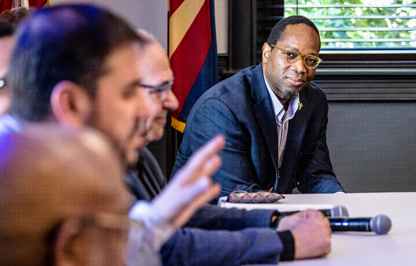
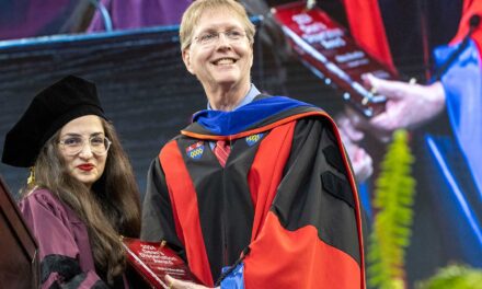
Associate Professor Michel Kinsy, director of ASU’s Secure, Trusted, and Assured Microelectronics, or STAM, Center listens during the academic panel on microelectronics training needs. Photographer: Charlie Leight/ASU News
Keynote speaker Dev Shenoy, principal director for microelectronics for the Office of the Under Secretary of Defense for Research and Engineering in the U.S. Department of Defense, agrees that building the workforce is vital.
“Workforce development and an increased emphasis on microelectronics education is critical for the U.S. to be successful in on-shoring semiconductor manufacturing,” Shenoy says. “The CHIPS and Science Act will foster the pipeline of talent through the Microelectronics Commons, for example, to strengthen the workforce where it is needed and bolster local economies where hubs and core facilities are located.”
In addition to the Department of Defense, other government entities present included the U.S. Department of Commerce and its National Institute of Standards and Technology, the CHIPS Act implementation team and the Defense Advanced Research Projects Agency, or DARPA.
“We want to return leading-edge manufacturing to the U.S.,” says Jessica R. Nicholson, workforce policy advisor for the CHIPS Act. “To do that, we need to create an ecosystem of manufacturers and suppliers, equipment materials researchers and designers in processes, and build a trained workforce. The availability of these resources will drive innovation across the technological and industrial sectors.”
Among the other attendees were industry groups including Synopsys, Raytheon Technologies, Boeing, Siemens Government Technologies and BAE Systems. There was also representation from military organizations, including the DEVCOM Army Research Laboratory and the Air Force Research Laboratory.
National laboratories in attendance included Argonne National Laboratory, Pacific Northwest National Laboratory and Sandia National Laboratories.
In his presentation, Rick McCormick, a representative from the Microsystems Engineering, Science and Application Center at Sandia National Laboratories, alluded to the strong correlation between manufacturing and innovation, and the impact of student collaboration.
“The way we execute our mission is heavy partnering within the government and all kinds of companies,” he says. “Three-quarters of the projects have university partners associated with them, with one of our partners being ASU.”
All event participants agreed that higher education institutions play a crucial role in bridging the workforce gap in microelectronics, with universities including ASU, Northern Arizona University, University of Arizona, George Washington University and Morgan State University in attendance to discuss how opportunities through each school are preparing students to enter the workforce.
A key discussion surrounded how to engage more diverse populations, including members of minority groups, veterans and community college students. University participants also highlighted the importance of pathway programs and reaching students at a young age, with K-12 pipelines to guide students toward microelectronics during their early education, such as at engineering summer camps and at ASU Preparatory Academy.
Squires detailed current efforts including the Microelectronics and Nanomanufacturing Certificate Program — offered in partnership with Penn State, the University of California San Diego, Georgia Institute of Technology and Norfolk State University — to reach active military personnel and veterans with stackable credential certifications at four strategically-located regional partner sites.
The sites, which are located in Phoenix, Atlanta, San Diego and Norfolk, Virginia, will each offer the program in collaboration with one state university and one local community college. In Phoenix, this will include Rio Salado College and ASU.
“Students who go through this program can achieve the kind of certification that industry understands and values,” Squires says.
The workshop also featured an academic panel on microelectronics training needs and an industry panel on talent needs, in addition to a tour of ASU’s MacroTechnology Works in Tempe. Led by Zachary Holman, an associate professor of electrical engineering in the Fulton Schools, the tour explored the facility and its efforts in accelerating semiconductor, advanced materials and energy device research.
“The MacroTechnology Works facility is a very unique space that will be integral in building physical infrastructure and advancing research, in addition to providing opportunities for training, internships and partnerships,” Squires says.
Squires also noted that the recent launch of ASU’s School of Manufacturing Systems and Networks, part of the Fulton Schools, exemplifies the university’s efforts to address current and future challenges and provide a center of gravity across engineering disciplines to focus on efforts relating to manufacturing.
“This workshop and the engagement that it fostered highlight the sort of interactions that we want to be having on a regular basis around this important topic,” Kinsy says. “Our goal was to open the door for continued discussions, which I believe we have achieved.”
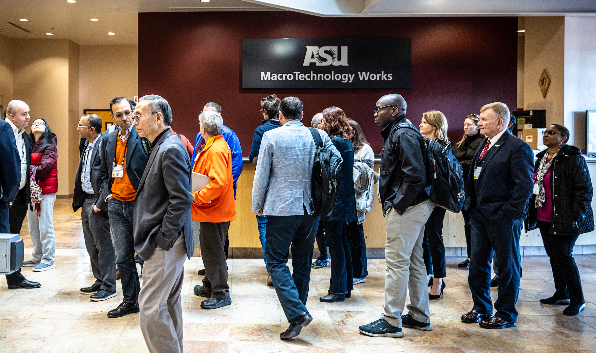
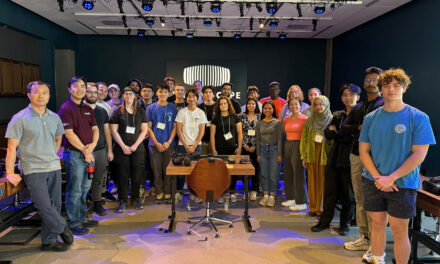
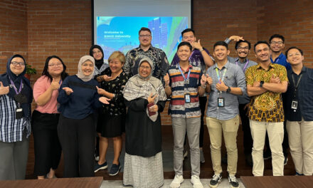
A group of dignitaries from government, universities, national research labs and private industry begin a tour of the MacroTechnology Works facility at ASU Research Park as part of the two-day Microelectronics Education and Workforce Development Workshop. Photographer: Charlie Leight/ASU News


