New nano-material combinations produce leap in infrared technology

ASU engineers are working on technological advances that promise to enhance infrared photodetection used in sophisticated weapons and surveillance systems, industrial and home security systems, medical diagnostics and night-vision equipment for law enforcement and driving safety.The advances could produce infrared photodetectors that require less power to operate, which would bring down costs of such technology as the automobile night-vision system pictured here. Photo courtesy of Daimler AG. Copyright: Daimler AG.
Posted: February 13, 2012
Arizona State University researchers are finding ways to improve infrared photodetector technology that is critical to national defense and security systems, as well as used increasingly in medical diagnostics, commercial applications and consumer products.
A significant advance is reported in a recent article in the journal Applied Physics Letters. It details discovery of how infrared photodetection can be done more effectively by using certain materials arranged in specific patterns in atomic-scale structures.
It’s being accomplished by using multiple ultrathin layers of the materials that are only several nanometers thick. Crystals are formed in each layer. These layered structures are then combined to form what are termed “superlattices.”
Photodetectors made of different crystals absorb different wavelengths of light and convert them into an electrical signal. The conversion efficiency achieved by these crystals determines a photodectector’s sensitivity and the quality of detection it provides, explains electrical engineer Yong-Hang Zhang.
The unique property of the superlattices is that their detection wavelengths can be broadly tuned by changing the design and composition of the layered structures. The precise arrangements of the nanoscale materials in superlattice structures helps to enhance the sensitivity of infrared detectors, Zhang says.
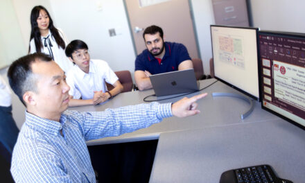
Zhang is a professor in the School of Electrical, Computer and Energy Engineering, one of ASU’s Ira A. Fulton Schools of Engineering. He is leading the work on infrared technology research in ASU’s Center for Photonics Innovation. More information can be found at the center’s Optoelectronics Group website.
Additional research in this area is being supported by a grant from the Air Force Office of Scientific Research and a new Multidisciplinary University Research Initiative (MURI) program established by the U.S. Army Research Office. ASU is a partner in the program led by the University of Illinois at Urbana-Champaign.
The MURI program is enabling Zhang’s group to accelerate its work by teaming with David Smith, a professor in the Department of Physics in ASU’s College of Liberal Arts and Sciences, and Shane Johnson, a senior research scientist in the ASU’s engineering schools.
The team is using a combination of indium arsenide and indium arsenide antimonide to build the superlattice structures. The combination allows devices to generate photo electrons necessary to provide infrared signal detection and imaging, says Elizabeth Steenbergen, an electrical engineering doctoral student who performed experiments on the supperlattice materials with collaborators at the Army Research Lab.
“In a photodetector, light creates electrons. Electrons emerge from the photodetector as electrical current. We read the magnitude of this current to measure infrared light intensity,” she says.
“In this chain, we want all of the electrons to be collected from the detector as efficiently as possible. But sometimes these electrons get lost inside the device and are never collected,” says team member Orkun Cellek, an electrical engineering postdoctoral research associate.
Zhang says the team’s use of the new materials is reducing this loss of optically excited electrons, which increases the electrons’ carrier lifetime by more than 10 times what has been achieved by other combinations of materials traditionally used in the technology. Carrier lifetime is a key parameter that has limited detector efficiency in the past.
Another advantage is that infrared photodetectors made from these superlattice materials don’t need as much cooling. Such devices are cooled as a way of reducing the amount of unwanted current inside the devices that can “bury” electrical signals, Zhang says.
The need for less cooling reduces the amount of power needed to operate the photodetectors, which will make the devices more reliable and the systems more cost effective.
Researchers say improvements can still be made in the layering designs of the intricate superlattice structures and in developing device designs that will allow the new combinations of materials to work most effectively.
The advances promise to improve everything from guided weaponry and sophisticated surveillance systems to industrial and home security systems, the use of infrared detection for medical imaging and as a road-safety tool for driving at night or during sand storms or heavy fog.
“You would be able to see things ahead of you on the road much better than with any headlights,” Cellek says.
The research team’s paper is reported on in the article “One giant leap for IR technology” on the LAB & FAB TALK website of Compound Semiconductor magazine.


