


Building the microelectronics manufacturing blueprint
ASU researcher Hongbin Yu leads team funded by $1.5 million DARPA grant to develop future microelectronics domestically

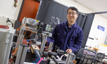
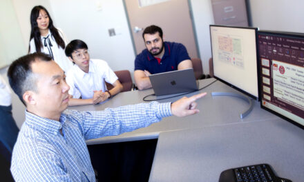
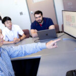
Electrical engineering Professor Hongbin Yu leads efforts at ASU for Phase 0 of DARPA’s Next-Generation Microelectronics Manufacturing program. The program aims to develop manufacturing techniques and facilities to produce 3D heterogeneously integrated microelectronics manufacturing systems in the U.S. with help from Deca Technologies, Microchip Technology and Siemens EDA. Photo by Erika Gronek/ASU
Semiconductor manufacturing’s return to the U.S. is a hot topic in light of policy actions such as the national CHIPS and Science Act and Arizona’s New Economy Initiative, which is bringing advanced technology jobs and manufacturing to Arizona. Along with these policies designed to spur domestic production of microelectronics, the U.S. Defense Advanced Research Projects Agency, or DARPA, is turning an eye to future needs.
DARPA launched the Next-Generation Microelectronics Manufacturing, or NGMM, program to develop systems to build new technology known as three-dimensional heterogeneously integrated, or 3DHI, microelectronics in the U.S. 3DHI microelectronics use a new architecture that can improve chip efficiency compared to current 2D and 3D designs. The program is part of DARPA’s larger Electronics Resurgence Initiative 2.0, which aims to make the U.S. a world leader in microelectronics.
Hongbin Yu, a professor of electrical engineering in the Ira A. Fulton Schools of Engineering at Arizona State University, leads a team funded by a $1.5 million grant through Phase 0 of the NGMM program — a six-month process in which researchers analyze manufacturing methods and turn their findings into recommendations known as exemplar microsystems. The recommendations aim to find the best way to create both a production facility and explore best practices for developing these microsystems.
“We’re thinking about how we can make the electrical connections reliable and cost-effective,” says Yu, a faculty member in the School of Electrical, Computer and Energy Engineering, part of the Fulton Schools. “We’re also looking at aspects of how to simplify the manufacturing process. We have to do it cheaply; if you spend $1 billion to make one 3DHI microsystem device, that doesn’t work.”
DARPA’s ultimate goal is to create a manufacturing facility, or multiple facilities if needed, that will enable industry, government and academia to create prototypes of 3DHI devices on a small scale across the U.S. This model will improve national security. The program’s later Phase 1 and Phase 2 projects will be active for five years and focus on implementing the methods Yu and his team have outlined in Phase 0.
Jamie Winterton, senior director of research strategy for ASU’s Global Security Initiative, or GSI, connects faculty members with relevant funding opportunities from the U.S. Department of Defense. She helped connect Yu with the research opportunity and oversaw the team that wrote the research proposal.
Winterton says she believes this project can benefit American microelectronics development in multiple ways.
“Even for prototyping, we rely on facilities in countries that may not have America’s best interests in mind,” she says. “The current process is set up for high-volume manufacturing of existing products, and it’s very challenging to test out new concepts in small batches. By creating a fully domestic, open-access research and development center, we can accelerate innovation in microelectronics and protect national security interests at the same time.”
New ideas for novel microelectronics
3DHI microsystems stack individual computer chips vertically instead of the traditional lateral design, which cuts down on resistance and increases efficiency by making the wires connecting the chips shorter.
Another novel feature of 3DHI systems is the connection of chips made from different material types, such as silicon carbide and gallium nitride, inside of one device. This enables the use of the best material for different applications depending on an individual chip’s purpose, such as processing, memory or radio communications, all assembled in a 3DHI package.
Assisting Yu with the efforts to create a manufacturing blueprint for these 3DHI devices are nine other faculty members from the School of Electrical, Computer and Energy Engineering, the School of Manufacturing Systems and Networks, the School for Engineering of Matter, Transport and Energy and the School of Computing and Augmented Intelligence, all part of the Fulton Schools. Their combined expertise spans the fields of electrical engineering, advanced manufacturing and electronics packaging thermal simulation.
Yu and his team also have graduate students taking part in the project by collecting necessary background information.
Electronics companies Deca Technologies, Siemens EDA and Microchip Technology are also involved in the NGMM program. For instance, Yu says Deca worked on high-density interconnect technology, a needed part of the 3DHI microsystems, in the last few years, making the company a valuable partner for such an effort.
The device recommendations the team plans to make seek to solve such problems as making the connections between chips in 3DHI devices as fast as possible, properly regulating heat generation, ensuring electrical signal integrity and maintaining computing power and data rate. All that information will provide significant benefits in supporting industry endeavors to continue to meet and exceed the standards set by Moore’s Law, which has driven the computing industry for more than 50 years.
Advancing Arizona microelectronics
Yu says one of his goals for ASU’s involvement in the NGMM project is to advance the microelectronics sector in Arizona.
“We’re putting together the toolsets and strategies to bring more companies to Arizona and to support existing companies,” he says.
Those involved also aim to engage ASU in more efforts related to the use of microelectronics to strengthen national security.
Kyle Elliott, a GSI proposal manager who helped oversee the proposal process for the NGMM project, says the project is among the first microelectronics programs GSI has been involved in. Considering its mission to address some of the world’s most pressing and sensitive security challenges, he sees Phase 0 as a great start for further collaborations with the Department of Defense.
“Phase 0 projects give you an inside path to the larger DARPA funding, which could be millions of dollars,” Elliott says.
His hope is that through the NGMM program and GSI’s other efforts, Phoenix will become a leading advanced manufacturing hub for the defense sector.
Yu also intends to continue his involvement in NGMM by applying for funding to do work for later phases of the project after his team completes Phase 0.
Winterton is optimistic that this is a great occasion for ASU researchers to showcase their knowledge and skills.
“We have the opportunity to share our institutional expertise in microelectronics in a way that will directly impact national security,” she says. “Six months is a very short period of time, but this team has the chops to produce some powerful and impactful recommendations for the next phases. I can’t wait to see what they come up with.”
Faculty members from the Fulton Schools involved in the NGMM project include School of Computing and Augmented Intelligence Associate Professor Giulia Pedrielli; School of Electrical, Computer and Energy Engineering Professor Christopher Bailey, Associate Professors Deliang Fan, Jennifer Kitchen, Jae-sun Seo and George Trichopoulos and Assistant Professor Ahmed Alkhateeb; School for Engineering of Matter, Transport and Energy Associate Professor Robert Wang; and School of Manufacturing Systems and Networks Director and Professor Binil Starly.


