


Semiconductor certificate moves students from lab to fab
New ASU graduate program supports industry expansion

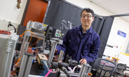
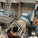
Above: Several new semiconductor manufacturing facilities, such as Intel's Fab 42 in Chandler, Arizona, are increasing regional demand for technical talent. To support this growth, ASU engineering faculty members have coordinated with industry managers to develop a new one-year certificate for current graduate students and those considering a related university graduate program. Photo courtesy of Intel
A global shortage of computer chips is disrupting the production of goods ranging from appliances to automobiles. Fully catching up with demand may take a year or more, but the semiconductor industry is already responding by expanding its manufacturing capacity. As part of this effort, the Phoenix metropolitan area is an emerging locus for new fabrication plants, or “fabs.”
Intel recently announced the construction of two additional fabs at its campus in the city of Chandler, Arizona, adding 3,000 new jobs when they open in 2024. Simultaneously, Taiwan Semiconductor Manufacturing Company has started construction on a north Phoenix fab that will create up to 1,900 new jobs when it opens the same year as Intel’s new facilities. In the meantime, Samsung Electronics is still deciding whether to open a fab employing 1,800 people at one of two potential sites around Phoenix.
These industry giants are attracted to Arizona for several reasons, but key to their plans is the pipeline of technical talent emerging from the Ira A. Fulton Schools of Engineering at Arizona State University. Even so, the semiconductor industry is developing rapidly, and equipping new engineers to succeed in such a dynamic environment is a challenge for any educational institution.
Meeting that challenge is the purpose of a new Certificate in Semiconductor Processing program at the Fulton Schools. Launched during the Fall 2020 academic term, the 15-credit graduate-level course framework provides professional training in multiple aspects of chip production.
“We’re not saying our certificate students will become experts in photolithography or chemical vapor deposition,” says Terry Alford, a professor of materials science and engineering as well as associate director of the School for Engineering of Matter, Transport and Energy, one of the six Fulton Schools. “But they will understand the terminology and fundamentals of the semiconductor manufacturing process to a level that enables them to immediately engage with colleagues at a fab and get work done well.”
Alford initiated organizing the certificate program two years ago, and created the framework in collaboration with Michael Kozicki and Trevor Thornton, both professors of electrical engineering in the Fulton Schools. All three faculty colleagues have direct commercial experience in the semiconductor industry, and those connections played a crucial role in program development.
“More than two dozen of my PhD students and 60 or 70 of my master’s students work in the semiconductor industry,” Alford says, noting that Kozicki and Thornton possess similar professional networks. “These people include hiring managers at Intel, for example, and we drew directly on what they told us they need when we designed the content of this certificate.”
At the heart of program are three core courses: Advanced Silicon Processing, an electrical engineering course; Design Engineering Experiments, an industrial engineering course; and Advanced Materials Characterization, a materials science and engineering course. Alford says this combination provides the foundation upon which students build their practical understanding of semiconductor fabrication work.
Beyond the core courses, all certificate program students choose two electives from among 11 options. Doing so makes the most of their current knowledge and supports the development of areas in which they want or need additional depth.
“People can customize this certificate experience according to their future goals,” Alford says. “If someone has an electrical engineering background, they already know solid-state devices. So, perhaps they’ll want to take an industrial engineering elective in statistical analysis to learn more about yield enhancement. Alternatively, they can take an elective to better understand cleanroom operations.”
The program’s adaptability extends to its delivery format. Access to expensive equipment, cleanrooms and other physical aspects of the semiconductor fabrication process might seem mandatory, but extensive curricular innovation during the pandemic now means that any of the courses can be completed on campus or online.
The new certificate is open to current Fulton Schools graduate students as well as to undergraduates participating in the accelerated 4+1 bachelor’s and master’s degree program. But Alford says this platform also serves as an invitation to current technology industry professionals who may be considering a return to university. He adds that the same is true of students who have completed an undergraduate degree in chemistry or physics and now want to enhance their marketability.
“If someone applies to this new certificate program, they can also apply, for example, to the online materials science and engineering master’s degree program. And they can do both for just one application fee,” Alford says. “Then, when they complete their certificate, they can step away, if they choose. They are not committed to do anything else. But we fully expect the certificate coursework will encourage people to continue their education and apply those same credits to completing their graduate engineering degree.”
Alford points out that the value of this certificate is not restricted to chip manufacturing. He says the program also supports the needs of equipment manufacturing — from aircraft to air conditioners — in which semiconductors are central to production.
“These businesses need good process engineers at their sites,” he says. “These are the people who communicate with the fabs to ensure successful technology transfer, and a lot of expensive decisions are based on this kind of expertise. So, the application of the new certificate is quite far-reaching.”


