DOE SunShot Initiative powers up ASU solar research projects
Two new solar research projects at Arizona State University will receive funding from the U.S. Department of Energy, the SunShot Initiative announced today. Both projects, funded under the Small Innovative Projects in Solar (SIPS) program, have the potential to dramatically reduce solar energy production costs.
The SunShot Initiative is designed to accelerate the market competitiveness of solar energy by targeting production cost reductions and increased solar deployment, with a 2020 target cost for utility-scale solar technologies that is roughly equal to electricity generation from fossil fuels.
Unconventional Tandem System
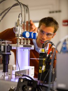
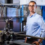
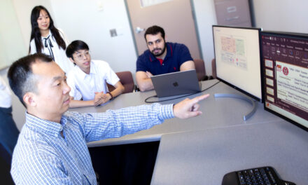
ASU Assistant Professor Zachary Holman. Photographer: Photographer: Jessica Hochreiter/ASU
Current photovoltaic modules have efficiencies of about 15-20 percent. Principal Investigator Zachary Holman, an ASU assistant professor, and Co-investigator Roger Angel, a Regents’ Professor at the University of Arizona, have proposed using an unconventional, tandem system to raise efficiency to greater than 30 percent. The new configuration is expected to open the door to manufacturing future tandem modules and bring solar energy production costs well below the DOE SunShot goal of $0.06 per kilowatt hour.
In conventional, single-junction silicon photovoltaic modules, infrared photons are efficiently converted into electricity, but much of the energy carried by visible photons is lost as waste heat. The proposed technology aims to remedy this by splitting the solar spectrum, directing infrared photons to a silicon solar cell, and directing visible photons to a gallium arsenide (GaAs) solar cell that is better suited to this energy range.
At the heart of the technology is a “PVMirror” — a silicon photovoltaic module that incorporates a spectrum-splitting optical coating and that is bent into a parabolic trough. The optical coating transmits infrared photons to the silicon cells while reflecting visible photons. Because the PVMirror is curved, the reflected photons arrive at a common focus, at which a GaAs solar cell is placed. This design has significant technological advantages over other tandem photovoltaic designs: the sub-cells do not need to be current matched, lattice matched, or process compatible, and the tandem converts some diffuse light (in addition to direct light) to electricity.
“We believe this SunShot project will allow us to demonstrate the first 30-percent-efficient silicon-based tandem mini-module within one year. We’re excited because this represents a significant bump above the present state of the art and the technology has commercial potential,” says Holman.
Loss and cost analyses based on data gathered during the project will reveal technological and market opportunities and risks for future PVMirror tandem module development.
Holman is an expert in photovoltaics and silicon solar cells in particular; Angel is an expert in optics and concentrators. With their complementary expertise, the team will fabricate solar cells, construct PV Mirrors, measure their efficiency outdoors on a sun tracker, and analyze the potential of the technology to break open a new photovoltaic market.
Silicon Wafer Technology
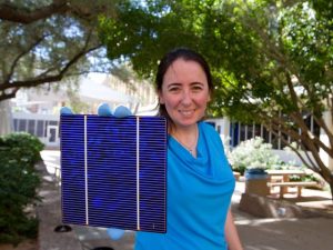
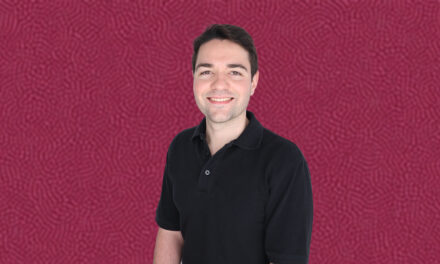
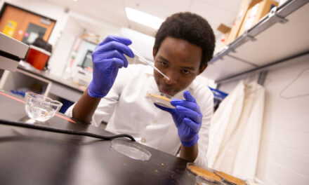
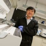
ASU Assistant Professor Mariana Bertoni. Photographer: Jessica Hochreiter/ASU
Principal Investigator Mariana Bertoni, an ASU assistant professor, has proposed a modified technique, sound-assisted low temperature (SALT) spalling, to peel a wafer from a silicon block by applying a tensile stress at low temperatures, as a method of eliminating kerf loss — the amount of material “lost” in the cutting process.
Kerf losses are associated with any type of cutting or sectioning of materials. Sawdust is an example of the kerf loss when sawing a piece of wood. In classical wire sawing technologies, kerf loss can equal to the thickness of the silicon wafers.
The proposed SALT process eliminates traditional abrasive slurries, wires, and multiple cleaning steps while doubling the yield of a silicon ingot. The idea is to precisely engineer the stress applied to layers in order to spall thicker wafers, control the fracture front to ensure high quality surfaces, and rely on low temperature processes to minimize unwanted decrease of carrier lifetime — an important indicator of substrate quality.
“The key challenges are to maintain the silicon quality during the process as well as controlling the motion of the fracture front. If we can achieve this we will have a game changing technology in our hands with untapped potential beyond silicon,” says Bertoni.
SALT technology, combined with state-of-the-art manufacturing, has the transformative potential to achieve highly efficient, lightweight and inexpensive solar models at far below current industry costs.
Bertoni is an expert in defect engineering of solar cell materials, transparent conducting oxides, defects in semiconductors, synthesis, growth and deposition of semiconductors, electrical and optical characterization, X-ray microscopy and spectroscopy.
Media Contact
Terry Grant, [email protected]
480-727-4089
Ira A. Fulton Schools of Engineering


